This project was under the guidance of Prof. Suddhasatta Mahapatra, Department of Physics, IIT Bombay.
The Problem Statement
The over-arching goal was to create qubits using spin of a single electron of silicon and then perform basic qubit operations on them. This goal can be divided into two sub-goal : First, to be able confine single electron and second, to be able to control spin of the electron. My target was to complete the first sub-goal which is to confine a single electron in silicon.
For single electron confinement, potential barriers are required in all three dimensions which is called a nanodot. So the problem is equivalent to engineering controllable potential barriers such that the nanodot becomes a quantum dot i.e. quantization of energy occurs and single electron occupancy of the dot can be acheived. Generally, two types of barriers are used, first is band defined barriers and second is electrostatically defined barriers
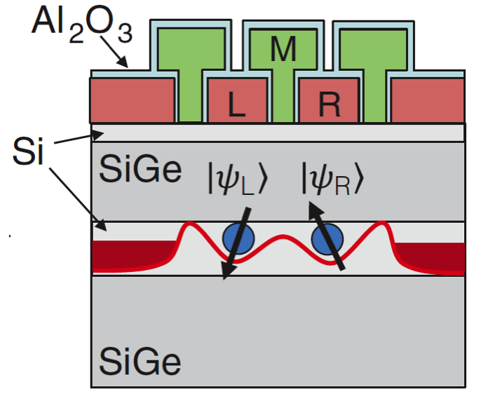 Fig 1: Cartoon of a Double Quantum Dot Architecture
The confinement in the z-direction is acheived using band defined barrier. As SiGe has a higher conduction band minimum than silicon (Si/SiGe is a type II heterostructure), z-direction confinement occurs when Si is sandwiched between SiGe layers as seen in the image above. The x- and y-directional confinment is acheived using metallic gates with a negative voltage which are fabricated on top of the device as denoted by the red squares in the above image. As silicon is a seminconductor it doesn’t have any conduction band electrons on its own. Hence a gate with a positive voltage is require to accumulate electrons at specific positions as denoted by the green squares in the above image. These gates are as small as few tens of nanometer and hence building them with accuracy is a challenge.
Fabrication of the device
The whole process is quite complicated and length, if interested you can find it in my master’s thesis here. However, just for excitement let me show you some cool images of the device while it was being fabricated
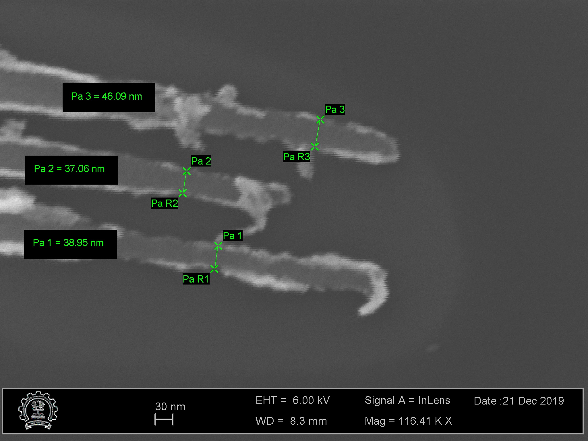 Fig 2: Example of a depletion gate (December 2019)
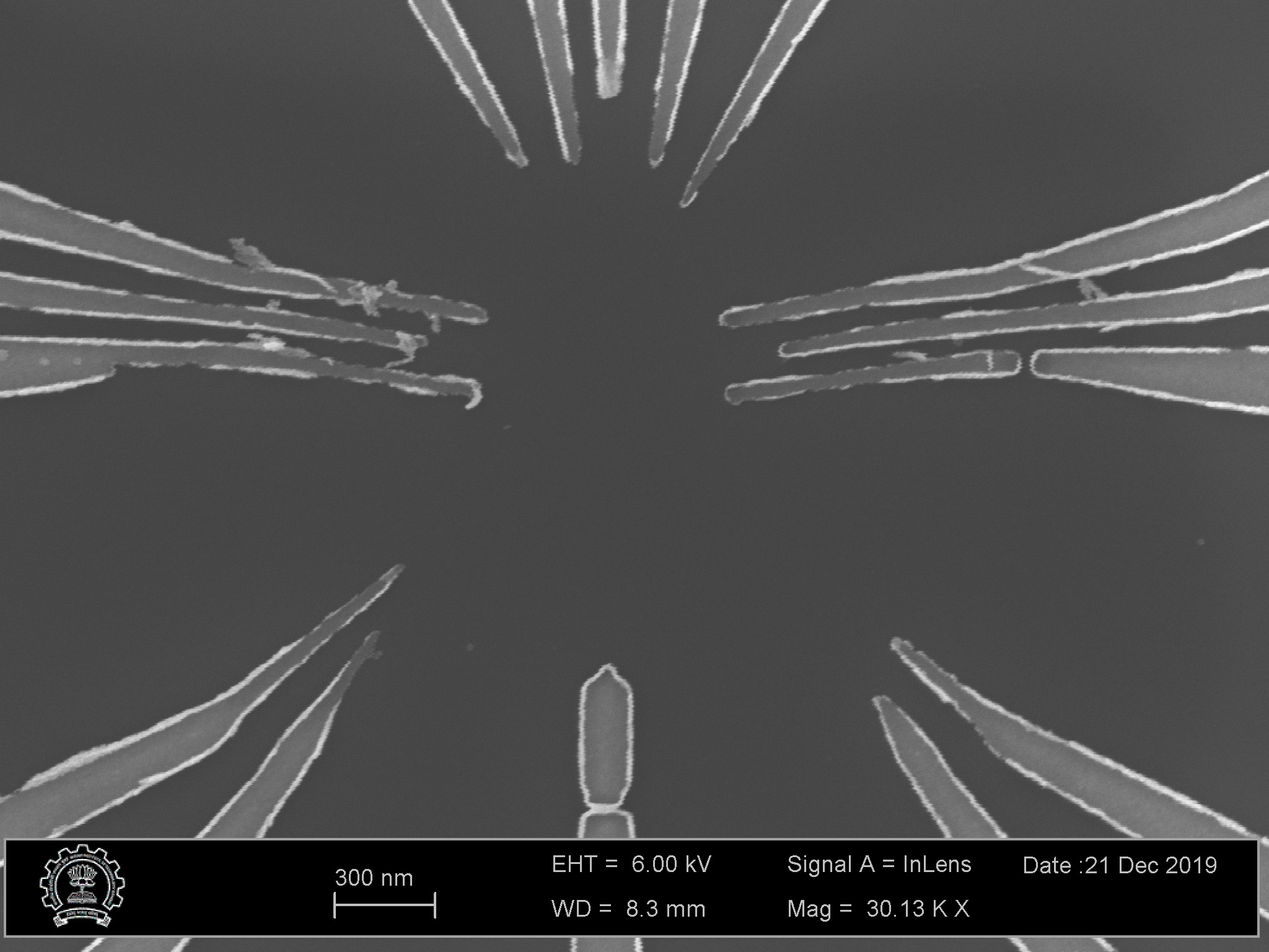 Fig 3: A failed run of building depletion gates (December 2019)
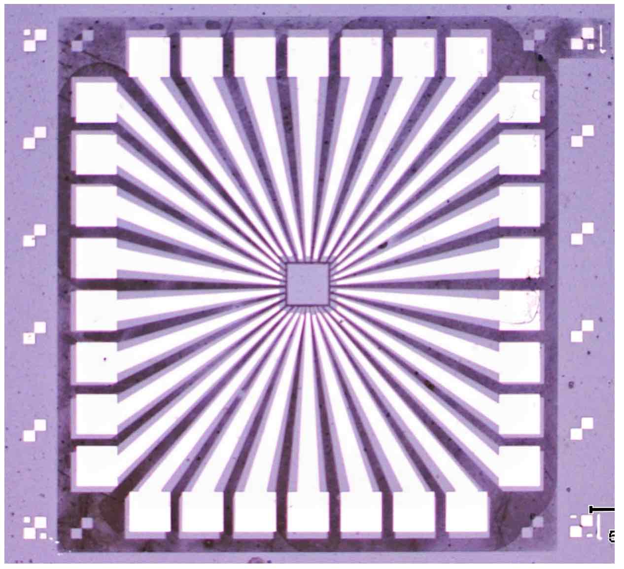 Fig 4: Partially ready device with only bondpads (August 2019)
These images were part of the intial optimisation runs. Unfortunately due to COVID19 the project was shortened by 3.5 months which were planned to be the final device fabrication months.